- 您现在的位置:买卖IC网 > Sheet目录323 > DSP56311EVM (Freescale Semiconductor)KIT EVALUATION FOR DSP56311
�� �
�
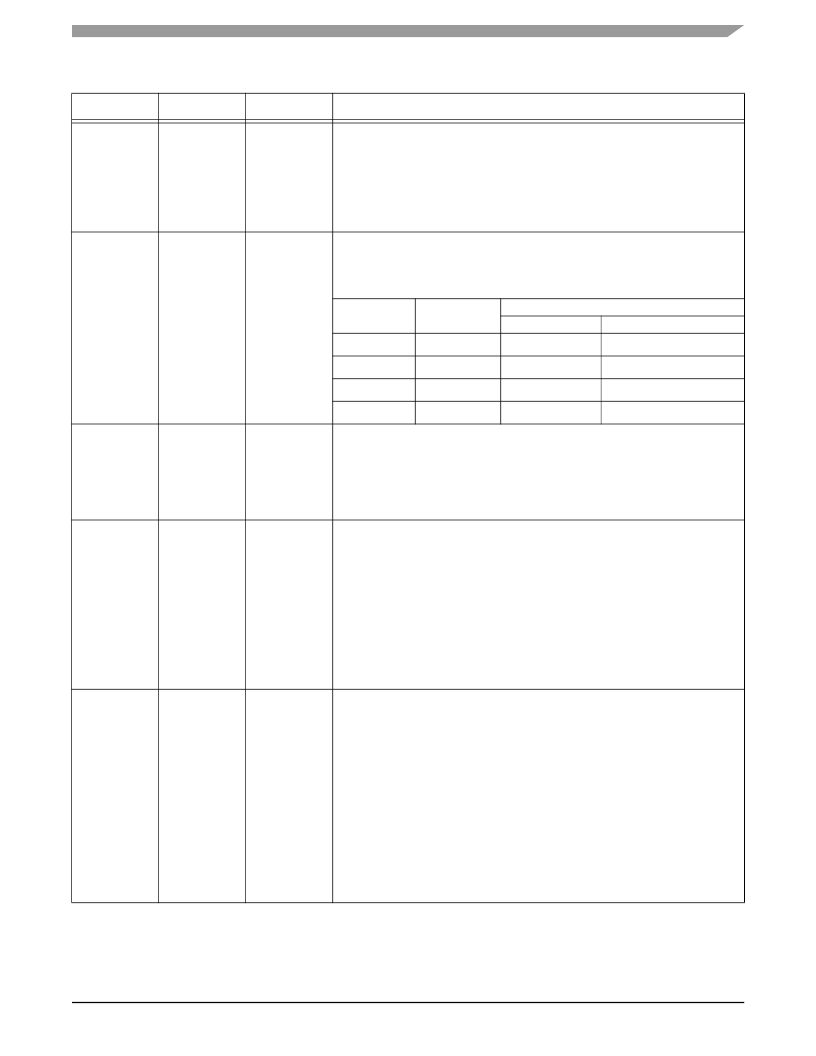
�ESSI� Programming� Model�
�Table� 7-4.� ESSI� Control� Register� B� (CRB)� Bit� Definitions� (Continued)�
�Bit� Number�
�9�
�Bit� Name�
�FSR�
�Reset� Value�
�0�
�Frame� Sync� Relative� Timing�
�Description�
�Determines� the� relative� timing� of� the� receive� and� transmit� frame� sync� signal�
�in� reference� to� the� serial� data� lines� for� word� length� frame� sync� only.� When�
�FSR� is� cleared,� the� word� length� frame� sync� occurs� together� with� the� first� bit�
�of� the� data� word� of� the� first� slot.� When� FSR� is� set,� the� word� length� frame�
�sync� occurs� one� serial� clock� cycle� earlier� (that� is,� simultaneously� with� the�
�last� bit� of� the� previous� data� word).�
�8–7�
�FSL[1–0]�
�0�
�Frame� Sync� Length�
�Selects� the� length� of� frame� sync� to� be� generated� or� recognized,� as� in�
���FSL1�
�0�
�0�
�1�
�1�
�FSL0�
�0�
�1�
�0�
�1�
�RX�
�word�
�word�
�bit�
�bit�
�Frame� Sync� Length�
�TX�
�word�
�bit�
�bit�
�word�
�6�
�SHFD�
�0�
�Shift� Direction�
�Determines� the� shift� direction� of� the� transmit� or� receive� shift� register.� If�
�SHFD� is� set,� data� is� shifted� in� and� out� with� the� LSB� first.� If� SHFD� is� cleared,�
����5�
�SCKD�
�0�
�Clock� Source� Direction�
�Selects� the� source� of� the� clock� signal� that� clocks� the� transmit� shift� register�
�in� Asynchronous� mode� and� both� the� transmit� and� receive� shift� registers� in�
�Synchronous� mode.� If� SCKD� is� set� and� the� ESSI� is� in� Synchronous� mode,�
�the� internal� clock� is� the� source� of� the� clock� signal� used� for� all� the� transmit�
�shift� registers� and� the� receive� shift� register.� If� SCKD� is� set� and� the� ESSI� is�
�in� Asynchronous� mode,� the� internal� clock� source� becomes� the� bit� clock� for�
�the� transmit� shift� register� and� word� length� divider.� The� internal� clock� is�
�output� on� the� SCK� signal.� When� SCKD� is� cleared,� the� external� clock� source�
�is� selected.� The� internal� clock� generator� is� disconnected� from� the� SCK�
�signal,� and� an� external� clock� source� may� drive� this� signal.�
�4�
�SCD2�
�0�
�Serial� Control� Direction� 2�
�Controls� the� direction� of� the� SC2� I/O� signal.� When� SCD2� is� set,� SC2� is� an�
�output;� when� SCD2� is� cleared,� SC2� is� an� input.�
�Note:�
�Programming� the� ESSI� to� use� an� internal� frame� sync� (that� is,�
�SCD2� =� 1� in� CRB)� causes� the� SC2� and� SC1� signals� to� be�
�programmed� as� outputs.� However,� if� the� corresponding�
�multiplexed� pins� are� programmed� by� the� Port� Control� Register�
�(PCR)� to� be� GPIOs,� the� GPIO� Port� Direction� Register� (PRR)�
�chooses� their� direction.� The� ESSI� uses� an� external� frame� sync� if�
�GPIO� is� selected.� To� assure� correct� operation,� either� program� the�
�GPIO� pins� as� outputs� or� configure� the� pins� in� the� PCR� as� ESSI�
�signals.� The� default� selection� for� these� signals� after� reset� is� GPIO.�
�This� note� applies� to� both� ESSI0� and� ESSI1.�
�DSP56311� User’s� Manual,� Rev.� 2�
�Freescale� Semiconductor�
�7-21�
�发布紧急采购,3分钟左右您将得到回复。
相关PDF资料
DSPAUDIOEVMMB1E
BOARD MOTHER DSP563XX
DSPIC30F2010 DEVELOPMENT KIT
KIT DEV EMBEDDED C
DSTRM-KT-0181A
DSTREAM DEBUG AND TRACE UNIT
DSUT1CSU
SURGE SUPPR NETWORK W/GROUND
DTEL2
SURGE SUPPRESSOR PHONE RJ11/RJ45
DV003001
PROGRAMMER PICSTART PLUS 16C/17C
DV164035
MPLAB ICD3 IN-CIRC DEBUGGER
DV164039
KIT DEV PIC24FJ256DA210
相关代理商/技术参数
DSP56311EVMIG_D
制造商:未知厂家 制造商全称:未知厂家 功能描述:DSP56311EVMIG DSP56311EVM Sample Code
DSP56311EVMUM
制造商:未知厂家 制造商全称:未知厂家 功能描述:DSP56311 Evaluation Module Hardware Reference Manual
DSP56311FACT
制造商:未知厂家 制造商全称:未知厂家 功能描述:DSP56311 Higher performance programmable DSP for demanding voice and data applications
DSP56311UM
制造商:未知厂家 制造商全称:未知厂家 功能描述:DSP56311 24-Bit Digital Signal Processor Users Manual
DSP56311UMAD
制造商:未知厂家 制造商全称:未知厂家 功能描述:DSP56311 Users Manual Addendum
DSP56311VF150
功能描述:数字信号处理器和控制器 - DSP, DSC 150Mhz/300MMACS 150Mhz EFCOP RoHS:否 制造商:Microchip Technology 核心:dsPIC 数据总线宽度:16 bit 程序存储器大小:16 KB 数据 RAM 大小:2 KB 最大时钟频率:40 MHz 可编程输入/输出端数量:35 定时器数量:3 设备每秒兆指令数:50 MIPs 工作电源电压:3.3 V 最大工作温度:+ 85 C 封装 / 箱体:TQFP-44 安装风格:SMD/SMT
DSP56311VF150B1
功能描述:数字信号处理器和控制器 - DSP, DSC 24 BIT DSP
RoHS:否 制造商:Microchip Technology 核心:dsPIC 数据总线宽度:16 bit 程序存储器大小:16 KB 数据 RAM 大小:2 KB 最大时钟频率:40 MHz 可编程输入/输出端数量:35 定时器数量:3 设备每秒兆指令数:50 MIPs 工作电源电压:3.3 V 最大工作温度:+ 85 C 封装 / 箱体:TQFP-44 安装风格:SMD/SMT
DSP56311VF150R2
功能描述:数字信号处理器和控制器 - DSP, DSC 24 BIT DSP RoHS:否 制造商:Microchip Technology 核心:dsPIC 数据总线宽度:16 bit 程序存储器大小:16 KB 数据 RAM 大小:2 KB 最大时钟频率:40 MHz 可编程输入/输出端数量:35 定时器数量:3 设备每秒兆指令数:50 MIPs 工作电源电压:3.3 V 最大工作温度:+ 85 C 封装 / 箱体:TQFP-44 安装风格:SMD/SMT